

 News Center
An “Elemental Scan” of a Single Wafer
Introduction:
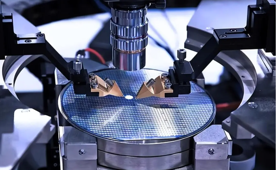
In a semiconductor materials analysis laboratory, a wafer is loaded into a femtosecond laser ablation system. The laser scans the surface point by point at extremely high speed, acquiring signals from over 100,000-pixel points across tens-of-millimeters-scale region, ultimately mapping the two-dimensional distribution of multiple trace elements via ICP-MS.
This is not science fiction, but a typical application of femtosecond laser ablation–inductively coupled plasma–mass spectrometry (fsLA-ICP-MS) technology in the semiconductor domain. Unlike conventional methods, this technique requires no wafer dissolution and no complex sample preparation, completing high-sensitivity elemental imaging directly through “solid sampling.”
Semiconductor Materials Elemental Imaging: What Exactly Needs to Be Seen?
Narrowing down the technology to practical applications, semiconductor industry requirements for elemental mapping fall into three well-defined categories:
1.Doping Uniformity Verification:
Is the distribution of dopant elements uniform after epitaxy or ion implantation? Are there radial gradients or circumferential striations? Rapid feedback is essential for process parameter optimization, which relies on full-wafer-scale elemental distribution maps.
2.Metal Contamination Traceability:
Transition metals such as Fe and Cu severely degrade semiconductor device performance. Once surface screening confirms Cu contamination, the next priority is pinpointing its location. Spatial patterns – discrete spots (particulate falloff from equipment), linear traces (conveyor abrasion), or widespread planar coverage (residual chemical fluid) – directly identify the responsible manufacturing stage.
3.Defect Correlation Analysis:
For haze defects, slip lines or anomalous discoloration on wafer surfaces, elemental mapping quantifies compositional divergence between defective and intact regions. The technique must preserve authentic signals across sharp defect boundaries without artificially blurring edges during measurement.
Though distinct, all three applications impose identical core requirements on mapping systems: high analytical fidelity, efficiency, and large-area scanning capability.
Limitations of Conventional Distribution Characterization Methods
Currently adopted elemental analysis techniques in the semiconductor industry all feature notable shortcomings when meeting the above application demands:
Secondary Ion Mass Spectrometry (SIMS)
SIMS supports elemental mapping with submicron spatial resolution. However, its mapping efficiency is extremely low: sequential sputtering via focused ion beams requires excessive runtime to generate full-wafer elemental images. More importantly, severe matrix effects lead to drastically divergent sputtering yields across different elements, preventing direct comparison of signal intensities on a single specimen. The fidelity and reliability of quantitative distribution is questionable.
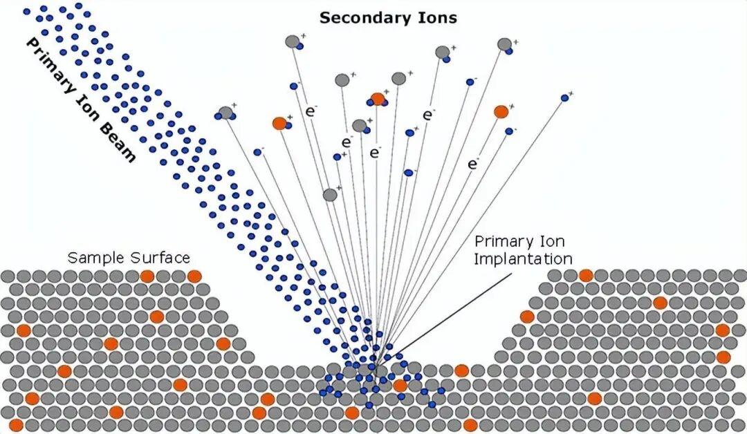
SIMS sputtering
TXRF/VPD-TXRF:
Widely used for semiconductor impurity testing, yet fundamentally a surface-averaging technique. Its millimeter-scale X-ray beam outputs average elemental concentrations across the irradiated area with no spatial distribution data. It can only confirm contamination exists rather than pinpoint its location to identify problematic production steps.
Solution-based ICP-MS:
Extremely high sensitivity but it requires digestion of wafer material into solution. All spatial information is permanently lost during dissolution, leaving only bulk average elemental content data.
This creates a core industry dilemma: conventional methods are either spatially blind, quantitatively unreliable, or prohibitively slow for mapping needs.
The Core Advantages of Matrix-Array Femtosecond Technology
Matrix-array femtosecond technology targets the above shortcomings via superior mapping fidelity and analytical efficiency.
1. “Cold Ablation” Preserves In-Situ Information
The femtosecond pulse (10-15 s) delivers instantaneous energy input before thermal conduction occurs within crystal lattices, vaporizing materials into nanometer-scale particles via cold processing. This “cold processing” characteristic means:
•Elements do not migrate: Thermal diffusion is eliminated, so e.g., Zn and other elements remain at their original positions without any signal loss or positional shift induced from thermal volatilization.
•Uniform response across all elements: Variations in elemental volatility are largely suppressed during femtosecond ablation. Comparably high-fidelity distribution maps for multiple elements can be acquired under identical experimental parameters for straightforward cross-comparison.
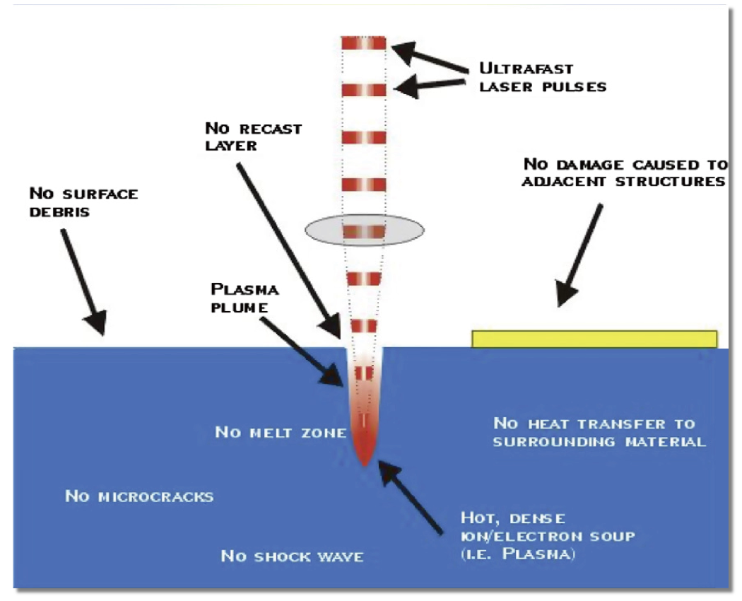
Femtosecond laser ablation
2. Matrix-Array Scanning Balances high resolution and high speed
Equipped with a 2D galvanometer scanner, the matrix-array femtosecond system rapidly deploys a large number of ablation points across the wafer scale. This design brings direct key benefits:
•High definition: The matrix-array spots can achieve continuous adjustment from μm to mm scales (minimum 1 μm). Small spot sizes resolve tiny defects while larger ones accelerate overall scanning; Simultaneously, high-density stitching of over 100,000 ablation points ensures that even millimeter-scale or smaller distribution anomalies cannot escape detection.
•High speed: Replacing slow conventional single-spot line-by-line scanning, the high-speed galvanometer rapidly jumps across the entire surface, significantly shortening wafer-scale imaging time and achieving true high-throughput surface scanning.
For routine semiconductor quality control, ultra-fine submicron resolution is rarely required; instead, rapid full-wafer screening to identify homogeneous or anomalous regions is prioritized. Array femtosecond scanning parameters hit this practical sweet spot with appropriate coverage range, speed and spatial precision.
3. Dual Optical Paths and Dual Objective Lenses
The same instrument supports both high-speed production-line screening and high-precision microscopic R&D tracing without trading off efficiency for resolution. When abnormal hotspots appear on distribution maps, there is no need to switch instruments — users switch to high-resolution microscopic analysis with one click on the same device, enabling a seamless workflow: full overview first, followed by targeted detailed inspection.
4. Integrated LIBS fills elemental detection gaps
A While fsLA-ICP-MS delivers excellent sensitivity, mass spectrometry is inherently limited for light elements including H, O and N. The built-in LIBS (Laser-Induced Breakdown Spectroscopy) module integrated into the system utilizes optical emission spectroscopy to directly collect characteristic plasma optical emission, bypassing ICP-MS detection to reliably quantify these light elements.
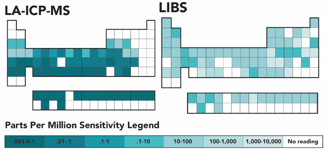
fsLA-ICP-MS and LIBS elemental coverage comparison
LIBS delivers unique supplementary imaging capability for critical semiconductor metrics such as oxygen distribution and hydrogen contamination that standard LA-ICP-MS cannot achieve. Spatial mapping of H, O and other light elements is no longer unattainable, enabling a complete imaging solution covering both light and heavy elements.
5. Stable transport of nanoparticles
Femtosecond ablation predominantly generates particles ranging from 10–200 nm, much finer than micrometer-sized particles from nanosecond ablation. Small particles have high transport efficiency and stability in the carrier gas, yielding more stable signals upon introduction into the ICP-MS.
In imaging results, this translates to reduced baseline noise and sharper feature boundaries. Measured intensities stay consistent across regions with identical elemental concentrations, while genuine compositional boundaries produce sharp signal transitions. Such favorable signal-to-noise performance is essential for distinguishing gradual diffused contamination from abrupt localized impurity spikes.
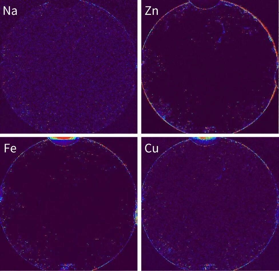
Wafer surface scanning imaging using fsLA-ICP-MS
Requirements for analytical instrumentation within the semiconductor industry can be summarized as four core criteria: higher speed, superior accuracy, simplified operation and intuitive data output. Thanks to its innovative physical principle that suppresses thermal artifacts via ultrashort laser pulses, femtosecond laser ablation concurrently fulfils these traditionally conflicting demands.
fsLA-ICP-MS is redefining the boundaries of semiconductor material characterization. Rather than replacing established techniques such as SIMS and TXRF, it delivers a superior solution in scenarios such as high-throughput screening, in-situ elemental mapping and rapid process feedback.
Copyright 2024 Shanghai CHEMLAB Instrument Co., Ltd. All Rights Reserved
Shanghai ICP Filing No.65656565