

 News Center
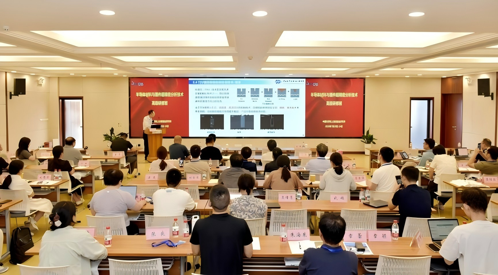
Recently, the Advanced Training Course on "Ultra-Precision Analytical Technologies for Semiconductor Materials and Devices" was successfully held at the Shanghai Institute of Ceramics, Chinese Academy of Sciences. Chemlab Instruments Co., Ltd. (Shanghai), as a domestic provider of high-end elemental analysis testing solutions, was invited to participate in this course and delivered a featured presentation at the event. This marks Chemlab's first formal appearance in the semiconductor materials field, signaling the company's strategic expansion from traditional geological analysis into national strategic industries such as semiconductors and new energy.
From Geoscience Foundations to New Frontiers in Materials
Femtosecond laser ablation–inductively coupled plasma–mass spectrometry (fsLA-ICPMS) has long been a core tool in geology and Earth science research – from rock dating and trace-element analysis of minerals, to in-situ quantitative analysis of Chang'e-6 lunar soil using extra-large spot sizes. This technology has proven its reliability and precision through rigorous geoscience applications.
As strategic industries such as advanced manufacturing, semiconductors, and new energy impose ever-higher demands on material purity and micro-scale characterization, this "geoscience power tool" is rapidly extending into materials science, leveraging its inherent advantages of micro-damage, in-situ analysis, and high resolution to become a new method for direct solid material analysis.
During the course, Chemlab's engineer explained: "Geological samples are often complex in composition and diverse in morphology, imposing extremely stringent requirements for in-situ micro-analysis. It is precisely this technical capability, honed under such demanding conditions, that enables the Genesis femtosecond laser system to handle the characteristics of semiconductor materials – high purity, micro-/nano-scale features, and thermal sensitivity – with remarkable ease."
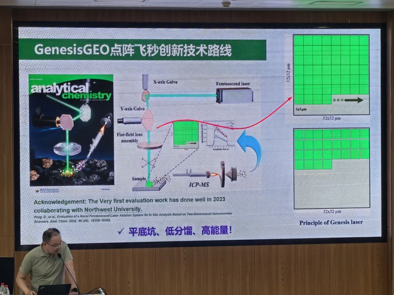
Special Report on Materials by Chemlab
Authoritative Platform Witnesses Technology "Crossover"
This advanced training course was organized by the Shanghai Institute of Ceramics, Chinese Academy of Sciences, and selected 69 official participants from hundreds of applicants nationwide. It brought together top scholars including Academician Chen Lidong of the Chinese Academy of Sciences, Professor Yang Shuming of Xi'an Jiaotong University, Professor Tan Pingheng of the Institute of Semiconductors, CAS, as well as key industry players such as JCET and Anji Microelectronics.
On such a high-profile academic platform, Chemlab made its debut as a provider of materials analysis solutions, systematically presenting the complete capability map of fsLA-ICPMS technology as it transitions from its geological "home turf" to the new "arena" of semiconductor materials testing.
Proven Performance in Cross-Sector Applications
The femtosecond laser (pulse width 10-15 seconds) employed by the Genesis system is fundamentally different from conventional nanosecond lasers. Through multi-photon absorption and tunnel ionization, femtosecond laser ablation induces Coulomb explosion, resulting in an extremely small heat-affected zone and finer, more uniform ablation particles. Built on this technological foundation, fsLA-ICPMS delivers three core capabilities for materials analysis: <1 µm spatial resolution, ppt-level detection limits, and minute-scale analysis speed. Furthermore, the matric-array femtosecond laser ablation technology has already achieved several breakthrough applications in the materials field:
·Impurity analysis of SiC wafers
·Wafer mapping imaging
·Failure analysis of metallic materials
·Impurity analysis of high-purity materials
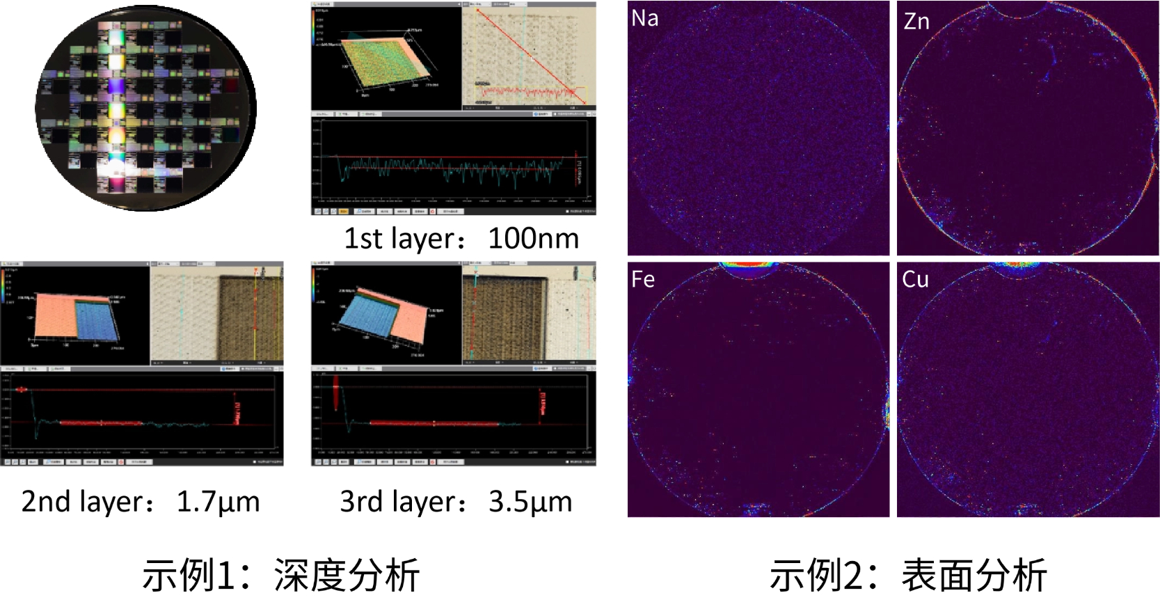
Case Studies in Material Analysis by Chemlab
From Research Tool to Production Tool
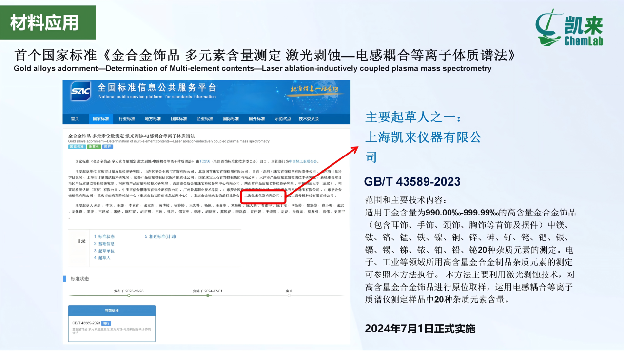
Notably, Chemlab, as a major drafting unit, participated in the development of GB/T 43589-2023 "Gold alloy jewellery – Determination of multi-element content – Laser ablation–inductively coupled plasma mass spectrometry", which officially came into effect in July 2024 – marking China's first national standard for LA-ICPMS. From participating in national standard-setting to launching dedicated testing systems for the semiconductor industry, the Genesis series is steadily evolving along the pathway of "research tool → engineering quality control tool → in-line production tool."
Chemlab is now offering a trial testing program for semiconductor customers, covering wafer-type samples such as SiC, GaN, and InP, as well as material testing services for high-purity quartz, high-purity graphite, ceramic substrates, battery electrodes, and more. This is not merely a market promotion, but also an opportunity for the industry to experience first-hand the value of femtosecond laser technology – when a well-established analytical method from the geosciences "crosses over" to the front lines of semiconductor quality control, it may bring not just an update in testing methods, but a fundamental upgrade in the entire quality control logic.
Future Outlook
As the semiconductor industry advances toward higher integration and more advanced process nodes, the demands for material purity and defect control are becoming increasingly stringent. Chemlab will continue to deepen its expertise in femtosecond laser ablation technology, with the strategic direction of "transforming research tools into production tools," providing independently developed and controlled testing technology support for key industries including advanced manufacturing, semiconductors, and new energy.
Limited-Time Offer: Free Semiconductor Sample Testing Experience!
To enable more semiconductor companies to experience firsthand the capabilities of domestically developed femtosecond laser testing technology, Chemlab is now launching the "Semiconductor Materials Free Testing Experience Program":
Free Testing Scope
·Wafer-type: Surface/bulk metal impurity analysis for SiC, GaN, InP, GaAs, silicon-based wafers, etc.
·High-purity materials: Trace impurity analysis for high-purity quartz, high-purity graphite, high-purity metals, Al2O3, etc.
·Composite materials: Micro-scale elemental distribution analysis for ceramic substrates, packaging materials, sputtering targets, battery electrodes, etc.
·Failure samples: Elemental source tracing for defective areas, depth profiling of coatings, inclusion analysis.
What You Will Receive
One-on-one technical consultation with professional engineers
Comprehensive elemental content testing report
Elemental distribution imaging maps (depending on sample requirements)
Customized testing solution recommendations
⏰ Starting now, 60 free testing slots are available on a limited-time basis. Applications will be evaluated, with priority given to high-quality research projects. Slots are limited and will be allocated on a first-come, first-reviewed basis.
Sample Submission for Testing:
Tel:021-58955763
Tel:15900900645
Copyright 2024 Shanghai CHEMLAB Instrument Co., Ltd. All Rights Reserved
Shanghai ICP Filing No.65656565