

 News Center
Following the successful release of the GenesisSEMI Auto fully automatic wafer contamination analysis system in May 2026, Shanghai Chemlab Semiconductor Division is once again making a move – the laboratory flagship platform GenesisSEMI Lab is currently in the finalization phase and will be unveiled soon!
GenesisSEMI Lab is not just the "laboratory version" of GenesisSEMI Auto; it represents a leap in technological dimensions. For the first time, it introduces a CARS (Coherent Anti-Stokes Raman Scattering) technology module, forming a trinity analysis Matrix-Array fsLA-ICP-MS and LIBS, bringing full-spectrum characterization capabilities from inorganic elements to organic molecules to semiconductor materials research. GenesisSEMI Lab upgrades process development and failure analysis from traditional "total quantity inference" to "in-situ diagnosis."
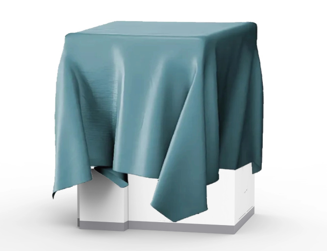
GenesisSEMI Lab
One Instrument, Three Perspectives
The core competitiveness of GenesisSEMI Lab lies in the deep integration and data fusion of three detection technologies. Each technology addresses different physicochemical properties of semiconductor materials, providing indispensable information dimensions.
01
fsLA-ICP-MS Module
fsLA-ICP-MS:The "All-Rounder" for Ultra-trace Element Analysis
Technical Highlights:fsLA-ICP-MS uses a femtosecond laser to generate extremely short pulses for precise ablation of the sample surface. The resulting aerosol particles are transported by a carrier gas to the ICP-MS for mass spectrometry analysis, achieving ultra-trace element detection sensitivity from ppb to ppt levels. Compared to traditional VPD-ICP-MS detection technology, its direct solid sampling capability avoids contamination risks from chemical reagents. It can not only detect metallic contamination on wafer surfaces but also perfectly addresses the inability of VPD technology to analyze bulk doping or elemental depth distribution.
Solid Standard Addition Method(SSAM)—— A precise quantitative scheme requiring no internal standard element:
·In-situ mixing of dual standard sample aerosols;
·Constant total ablation dose;
·Gradient concentration construction + extrapolation quantification
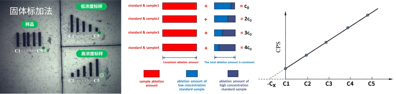
Schematic diagram of laser ablation solid standard addition method
The unique advantage of this method is that it achieves precise quantification without the need for matrix-matched solid reference materials, completely circumventing the methodological limitations caused by the scarcity of standard samples. At the same time, the entire process uses solid sampling, avoiding the cumbersome steps of digesting wafers into solutions as required by traditional solution standard addition methods, and eliminating secondary contamination and cross-contamination risks introduced by chemical reagents. Whether it is quantitative screening of metallic contamination on wafer surfaces or quantitative depth distribution analysis of bulk impurities, SSAM provides highly reliable data support.
In semiconductor application scenarios, the core value of combining fsLA-ICP-MS with SSAM technology is reflected in:
·Full Quantification of Ultra-trace Metal Impurities: Precise quantification of key metal impurities such as Fe, Cu, Ni, Cr, Na on wafer surfaces and in the bulk without the need for standard matching, with detection limits reaching ppt levels.
·Depth Distribution Analysis of Doping Elements: Accurately determines the vertical distribution curves of B, P, As, and other doping elements in silicon wafers with nanometer-level resolution, providing critical data for ion implantation process optimization and annealing process development.
02
LIBS Module
LIBS (Laser-Induced Breakdown Spectroscopy): The "Fast Hunter" for Light Elements and Halogens
LIBS is functionally complementary to fsLA-ICP-MS: ICP-MS has weak response to elements such as C, H, O, N, F, Cl, while LIBS, based on atomic emission spectroscopy, precisely fills this blind spot.
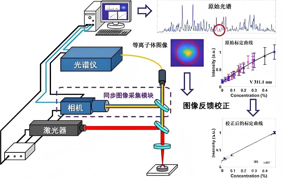
Although ICP-MS has unparalleled sensitivity for heavy metal elements, it has inherent limitations in detecting light elements (C, H, O, N) and halogens (F, Cl): these elements have high ionization energies, low ionization efficiency in the plasma, and are susceptible to polyatomic ion interferences (such as 12C16O+、28Si+), resulting in weak signals, high backgrounds, and difficult quantification. LIBS, based on the principle of atomic emission spectroscopy, detects characteristic spectral lines of excited-state atoms and has excellent response to these elements, precisely filling the elemental coverage gap of ICP-MS.
The GenesisSEMI Lab's ultrafast femtosecond laser engine, combined with a high-precision gas system and LIBS, requires no sample pretreatment, truly achieving "minute-level imaging and micron-level positioning," making it especially suitable for rapid screening and process monitoring.
03
CARS Module
CARS: The "Precision Locator" for Organic Contamination
GenesisSEMI Lab uniquely features the CARS (Coherent Anti-Stokes Raman Scattering) module.
GenesisSEMI Lab introduces the CARS analysis tool for the first time in the semiconductor industry. As a third-order nonlinear optical process, CARS uses two incident laser beams (pump beam and Stokes beam) to excite coherent Raman vibrations in the sample, and then the probe light scatters to generate an anti-Stokes signal. Its signal intensity is more than five orders of magnitude higher than traditional spontaneous Raman scattering, offering unique advantages of high chemical selectivity, high sensitivity, label-free, and non-destructive detection.
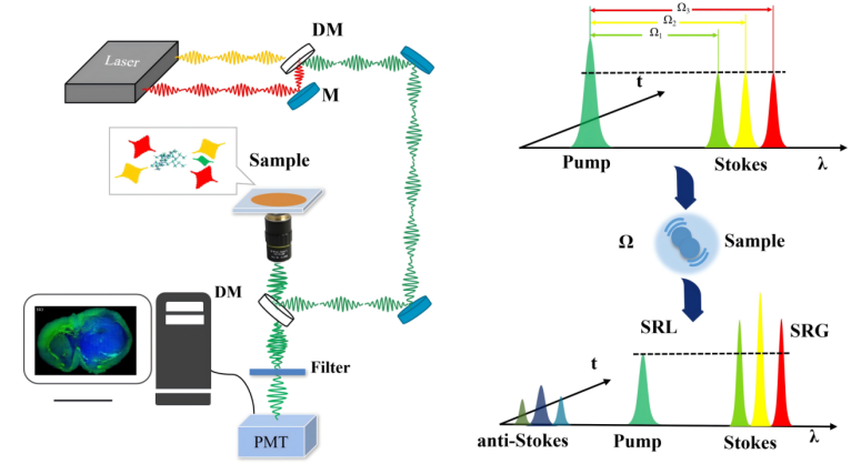
CARS system and principle
In semiconductor manufacturing, organic contaminants (such as photoresist residue, organic cleaning solutions, hydrocarbons, siloxanes, etc.) are "invisible killers" that severely impact device yield and reliability. However, existing organic contamination analysis methods have significant limitations:
·TD-GCMS (Thermal Desorption-Gas Chromatography Mass Spectrometry), as the current "gold standard" for organic contamination detection, has three major pain points: it can only measure total quantity, has a long analysis cycle, is destructive to the sample, and cannot provide spatial distribution. When yield anomalies occur on a wafer due to organic contamination, TD-GCMS can tell you "how much contamination" is present, but cannot tell you "where the contamination is located."
·CARS is a non-destructive technique that utilizes molecular fingerprinting characteristics. It can complete a full-wafer surface scan for organic contamination within minutes, precisely locating photoresist residues, cleaning solutions, hydrocarbons, etc., and tracing the source of contamination.
04
Full-Scenario Coverage: From Silicon-based to Wide Bandgap Semiconductors
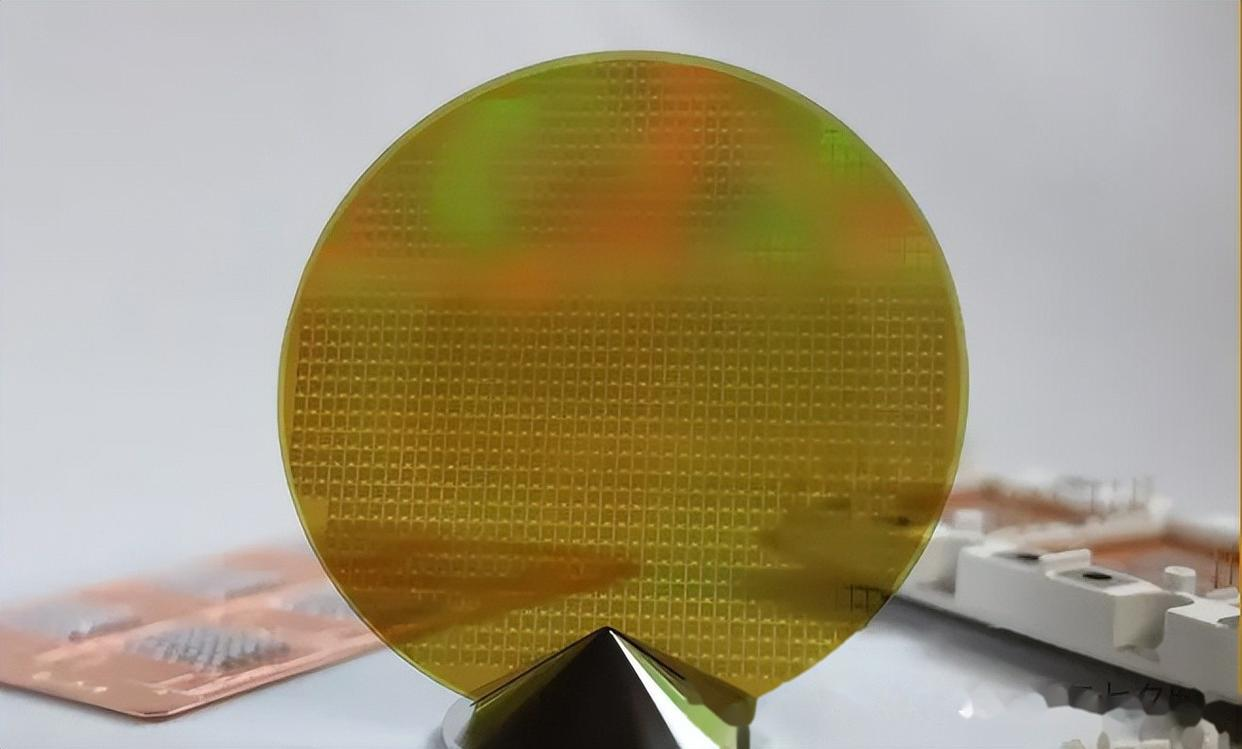
The GenesisSEMI Lab inherits the material compatibility advantages of the GenesisSEMI Auto, suitable not only for traditional silicon-based wafers but also capable of direct multimodal analysis of next-generation semiconductor materials such as SiC, GaN, GaAs, InP, and graphite. The system is equipped with seven automatic measurement modes (calibration curve, full scan, point mode, line scan, area scan, depth profile, and bevel analysis), flexibly addressing diverse needs ranging from rapid screening to micro-area fine mapping.
05
Strategic Significance: From "In-line Quality Control" to "R&D Enablement"
·GenesisSEMI Auto = A powerful tool for in-line quality control on semiconductor production lines.
·GenesisSEMI Lab = A deep characterization platform for semiconductor R&D laboratories, process development centers, and failure analysis platforms.
The two products share the core femtosecond laser engine and algorithm system, ensuring seamless connectivity between R&D data and production line quality control data, shortening the process transfer cycle from laboratory to production line.
Summary:
The launch of GenesisSEMI Lab marks that Shanghai Chemlab Semiconductor Division has completed its dual-line product layout of "industrial in-line version + laboratory flagship version," providing a full-chain solution for semiconductor materials research, process development, and quality control.
Stay tuned for the official release. Early inquiries and appointments are welcome.
References
[1] Becker, J.S., Zoriy, M., et al. Laser ablation inductively coupled plasma mass spectrometry (LA-ICP-MS) in the semiconductor industry. Journal of Analytical Atomic Spectrometry, 2008, 23, 1275-1282.
[2] Koch, J., et al. Femtosecond laser ablation ICP-MS for depth profiling of semiconductor materials. Spectrochimica Acta Part B: Atomic Spectroscopy, 2008, 63, 1241-1248.
[3] Hahn, D.W., Omenetto, N. Laser-induced breakdown spectroscopy (LIBS) for semiconductor analysis: A review. Applied Spectroscopy, 2012, 66, 347-419.
[4] Galmed, A.H., et al. Depth profiling of semiconductor materials by laser-induced breakdown spectroscopy. Applied Physics B, 2011, 102, 779-785.
[5] Sorrentino, F., et al. Calibration-free laser-induced breakdown spectroscopy (CF-LIBS) for quantitative analysis of AlGaAs wafers. Molecules, 2022, 15, 2851.
[6] Li, Y., et al. Advances in Femtosecond Coherent Anti-Stokes Raman Scattering for Thermometry. Photonics, 2024, 11, 622.
[7] Crampton, K., et al. Enhancement of molecular coherent anti-Stokes Raman scattering with silicon nano-antennas. Nature Communications (PMC), 2024.
Copyright 2024 Shanghai CHEMLAB Instrument Co., Ltd. All Rights Reserved
Shanghai ICP Filing No.65656565