

 News Center
Preface
In May 2026, Shanghai ChemLab Instrument Co., Ltd. announced the upcoming release of GenesisSEMI Auto, the first flagship product of its Semiconductor Division.
Leveraging the company’s core matrix-array femtosecond laser ablation technology, this high-end analytical instrument is customized for industrial wafer inspection. Its launch marks a strategic transformation for ChemLab: from manufacturing general scientific research instruments to delivering dedicated industrial solutions for vertical sectors. The system will fill a critical gap in the domestic semiconductor industrial chain.
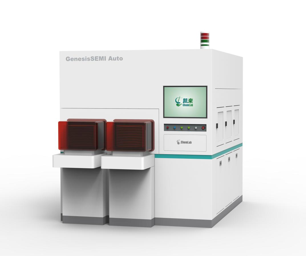
GenesisSEMI Auto
Addressing Industry Pain Points: Building the Next-Generation On-Site Quality Control Tools for Semiconductor Fabs
Currently, the semiconductor industry stands at the core of global technological competition. Restrictions on high-end computing power and advanced process technologies have accelerated the expansion of domestic production capacity for mature processes and third-generation semiconductors. Across the entire workflow from wafer fabrication to packaging and testing, the demand for precision measuring instruments such as thin film thickness gauges, surface defect detectors and Scanning Electron Microscopes (SEM) is growing exponentially.
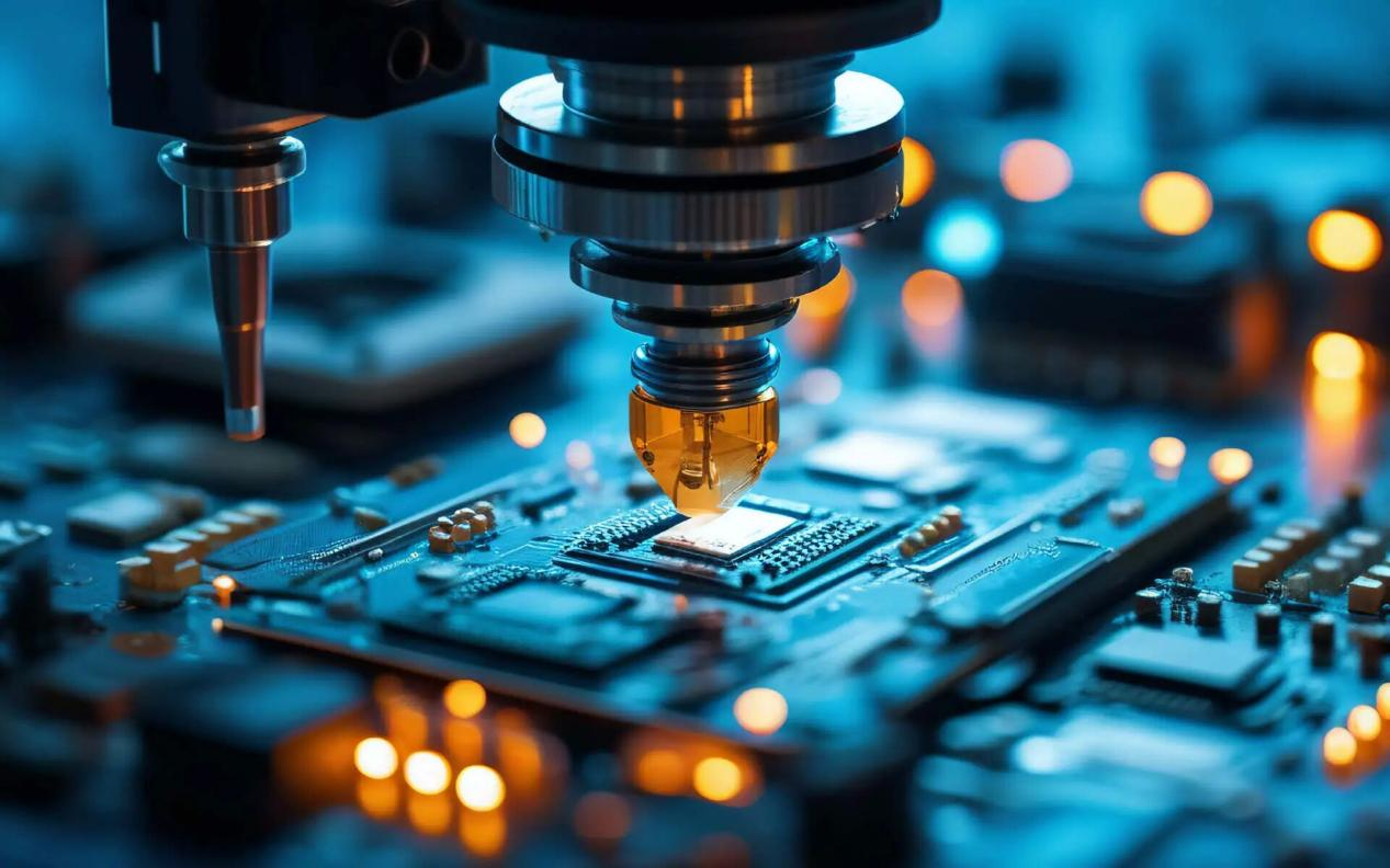
With the rapid iteration of semiconductor materials from traditional silicon-based substrates to wide-bandgap and compound semiconductors such as silicon carbide (SiC), gallium nitride (GaN), gallium arsenide (GaAs) and indium phosphide (InP), wafer contamination detection faces multiple critical challenges:
•Traditional VPD-ICP-MS is only applicable to silicon wafers decomposable by hydrofluoric acid. It fails to measure the content and uniformity of bulk dopant elements including boron (B), phosphorus (P) and arsenic (As), and is incompatible with next-generation compound semiconductor materials.
•High-end microanalysis equipment has long been dominated by overseas manufacturers, creating an urgent demand for domestic alternatives.
•Current testing solutions cannot simultaneously deliver high-throughput, automated on-line monitoring for both surface metallic contamination and bulk impurities.
Powered by its self-developed matrix-array femtosecond laser ablation technology with independent intellectual property rights, the Semiconductor Division of Shanghai ChemLab launches GenesisSEMI Auto. This system delivers a 24/7 unattended on-line analytical solution for semiconductor manufacturers. It serves as a full replacement for imported equivalent equipment and achieves technological independence in core bottleneck sectors.
Core Technical Advantages
GenesisSEMI Auto is a highly integrated, fully automated production-grade testing system featuring an innovative design with four core advantages:
1.Integrated large-size ultra-clean chamber
Different from conventional separate sample chambers, this design fully integrates the matrix-array femtosecond laser ablation system, femtosecond LIBS system and 5-axis precision motion stage inside one ultra-large clean chamber. Samples are completely isolated from the laboratory environment throughout the workflow under a constant atmosphere of ultra-high-purity inert gas, eliminating external contamination at the source.
2.Dual optical paths & solid standard addition method
Equipped with independently optimized dual optical paths and the patented Solid Standard Addition Method (SSAM), the system adopts in-situ aerosol mixing technology to achieve accurate quantification without internal standard elements, with industry-leading detection limits.
3.Ultrafast femtosecond laser engine
The system integrates a laser featuring an extremely short pulse width and a megahertz repetition rate. Two wavelength options are available: 343 nm for routine high-precision analysis and 257 nm for deep ultraviolet extreme performance. Combined with a high-speed scanner and high-precision gas circuit system, it generates stable nanoscale aerosol particles for direct introduction into ICP-MS. The workflow is greatly simplified, and prevents secondary contamination caused by chemical reagents.
4.Intelligent fully automatic wafer handling
Compliant with SEMI standard wafer specifications and integrated with an automatic Front Opening Unified Pod (FOUP) handling module, the system enables one-click unattended operation. Operators only need to place the wafer cassette at the loading port and set tasks; the system will automatically complete wafer transfer, positioning, multi-mode analysis and collection.
Full-scenario coverage: Compatible with the full spectrum of semiconductor materials Breaking material limitations, GenesisSEMI Auto performs impurity testing and depth profiling on conventional silicon wafers, as well as next-generation wafers made of SiC, GaN, GaAs, InP and graphene, with no complex sample pretreatment required.
Its software is deeply interconnected with ICP-MS, supporting seven automatic measurement modes: calibration curve acquisition, full-area scanning, point analysis, line scanning, area mapping, depth profiling and bevel analysis. It flexibly meets all testing requirements from rapid screening to high-resolution microscale mapping.
Strategic Significance: Domestic High-End Equipment Evolves from “Functional” to “Premium Performance”
The launch of GenesisSEMI Auto marks a milestone in Shanghai ChemLab’s strategic transformation from a supplier of general scientific research instruments to a manufacturer of high-end industrial semiconductor equipment. We have achieved full independent control across core technology, equipment manufacturing and on-site validation in fabrication scenarios. The system provides high-performance and highly reliable solutions for wafer manufacturers, driving a qualitative leap for domestic high-end semiconductor testing equipment.
Cooperation Invitation
Shanghai ChemLab sincerely invites partners from wafer manufacturing, semiconductor materials and testing equipment sectors for technical exchanges and on-site verification. Our R&D team provides customized product solutions tailored to practical application scenarios.
Moving forward, we will continue to launch dedicated complete sets of equipment and comprehensive solutions focusing on wafer contamination testing, as well as quality control for high-purity chemicals and electronic specialty gases. We aim to jointly formulate industry standards, expand the industrial ecosystem with all partners, and support the independent development of China’s semiconductor industry.
About Us
Headquartered at the Marine Science & Technology Pioneer Park, Lin-gang Special Area of China (Shanghai) Pilot Free Trade Zone, Shanghai ChemLab Instrument Co., Ltd. specializes in independent R&D and intelligent manufacturing of high-end analytical instruments. Based on our core matrix-array femtosecond laser ablation technology, we deliver a full range of comprehensive precision testing solutions, serving key sectors including high-end semiconductor manufacturing, cutting-edge scientific research and precision medical diagnostics.
Copyright 2024 Shanghai CHEMLAB Instrument Co., Ltd. All Rights Reserved
Shanghai ICP Filing No.65656565